(China (Mainland))


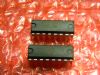
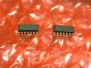
Product Summary
The CD4066B is a quad bilateral switch intended for the transmission or multiplexing of analog or digital signals.
It is pin-for-pin compatible with the CD4016B, but exhibits a much lower on-state resistance. In addition, the
on-state resistance is relatively constant over the full signal-input range.
The CD4066B consists of four bilateral switches, each with independent controls. Both the p and the n devices
in a given switch are biased on or off simultaneously by the control signal. As shown in Figure 1, the well of the
n-channel device on each switch is tied to either the input (when the switch is on) or to VSS (when the switch
is off). This configuration eliminates the variation of the switch-transistor threshold voltage with input signal and,
thus, keeps the on-state resistance low over the full operating-signal range.
The advantages over single-channel switches include peak input-signal voltage swings equal to the full supply
voltage and more constant on-state impedance over the input-signal range. However, for sample-and-hold
applications, the CD4016B is recommended.
Parametrics
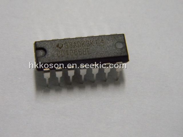
CD4066BE Parametrics:
Standard Package
25
Category
Integrated Circuits (ICs)
Family
Logic - Signal Switches, Multiplexers, Decoders
Series
4000B
Packaging
Tube
Type
Bilateral, FET Switches
Circuit
1 x 1:1
Independent Circuits
4
Current - Output High, Low
-
Voltage Supply Source
Dual Supply
Voltage - Supply
3 V ~ 18 V
Operating Temperature
-55°C ~ 125°C
Mounting Type
Through Hole
Package/Case
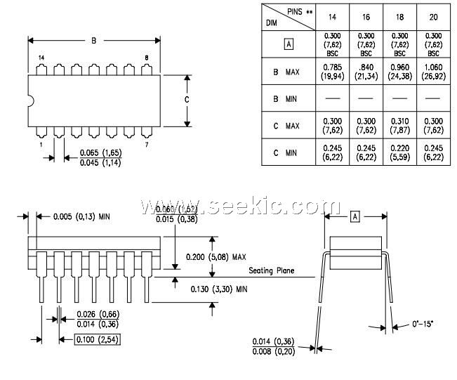
14-DIP (0.300", 7.62mm)
Supplier Device Package
14-PDIP
Dynamic Catalog
4000B
Other Names
296-2061-5
Features
CD4066BE Features:
- 15-V Digital or ±7.5-V Peak-to-Peak Switching
- 125-Ω Typical On-State Resistance for 15-V Operation
- Switch On-State Resistance Matched to Within 5 Ω Over 15-V Signal-Input Range
- On-State Resistance Flat Over Full Peak-to-Peak Signal Range
- High On/Off Output-Voltage Ratio: 80 dB Typical at fis = 10 kHz, RL = 1 kΩ
- High Degree of Linearity: <0.5% DistortionTypical at fis = 1 kHz, Vis = 5 V p-p,VDD ? VSS ≥ 10 V, RL = 10 kΩ
- Extremely Low Off-State Switch Leakage,Resulting in Very Low Offset Current and High Effective Off-State Resistance:
10 pA Typical at VDD ? VSS = 10 V, TA = 25°C
- Extremely High Control Input Impedance(Control Circuit Isolated From Signal Circuit): 1012 Ω Typical
- Low Crosstalk Between Switches: ?50 dB Typical at fis = 8 MHz, RL = 1 kΩ
- Matched Control-Input to Signal-Output Capacitance: Reduces Output Signal Transients
- Frequency Response, Switch On = 40 MHz Typical
- 100% Tested for Quiescent Current at 20 V
- 5-V, 10-V, and 15-V Parametric Ratings
- Meets All Requirements of JEDEC Tentative Standard No. 13-B, Standard Specifications for Description of “B” Series CMOS
Devices
Diagrams

| Image | Part No | Mfg | Description |  |
Pricing (USD) |
Quantity | ||||||||||||
|---|---|---|---|---|---|---|---|---|---|---|---|---|---|---|---|---|---|---|
 |
 CD4066BE |
Texas Instruments |
Analog Switch ICs Quad |
Data Sheet |
|
|
||||||||||||
|
CD4066BEE4 |
Texas Instruments |
Analog Switch ICs Quad |
Data Sheet |
|
|
||||||||||||