Product Summary
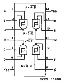
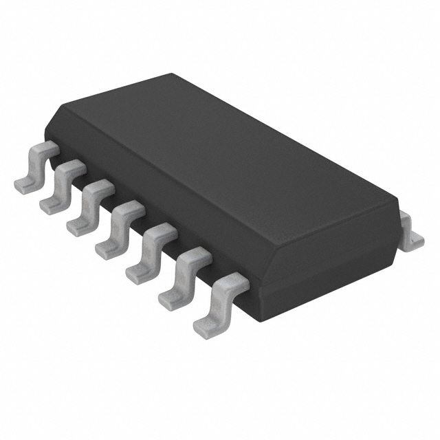
The CD4093BF is a Quad 2-Input NAND Schmitt Trigger. It consists of four Schmitt-trigger circuits. Each circuit functions as a 2-input NAND gate with Schmitttrigger action on both inputs. The gate switches at different points for positive and negative-going signals. The difference between the positive (VT+) and the negative voltage (VT-) is defined as hysteresis voltage (VH). The applications of the CD4093BF include Wave and pulse shapers, High-noise-environment systems, Monostable multivibrators, Astable multivibrators, NAND logic.
Parametrics
CD4093BF absolute maximum ratings: (1)DC supply voltage range, (VDD) voltage referenced to Vss terminal: -0.5V to 20V; (2)input voltage range, all inputs: -0.5V to Vdd+0.5V; (3)DC input current, any one input: ±10mA; (4) package thermal impedance: 80℃/W for E package; 86℃/W for M package; 76℃/W for NS package; (5)device dissipation per output transistor: 100mW; (6)operating temperature range: -55℃ to 125℃; (7)storage temperature range: -65℃ to 150℃; (8)lead temperature: 265℃.
Features
CD4093BF features: (1)schmitt-trigger action on each input with no external components; (2)hysteresis voltage typically 0.9 V at VDD=5V and 2.3V at VDD=10V; (3)noise immunity greater than 50%; (4)no limit on input rise and fall times; (5)standardized,symmeterical output characteristics; (6)100% tested for quiescent current at 20V; (7)maximum input current of 1μA at 18V over full package-temperature range; (8)5V,10V and 15V parametric ratings; (9)meets all requirements of JEDEC.
Diagrams

 |
 CD4000B |
 Other |
 |
 Data Sheet |
 Negotiable |
|
||||
 |
 CD4000BMS |
 Other |
 |
 Data Sheet |
 Negotiable |
|
||||
 |
 CD4001BC |
 Other |
 |
 Data Sheet |
 Negotiable |
|
||||
 |
 CD4001BCM |
 |
 IC GATE NOR BUFF QUAD 2IN 14SOIC |
 Data Sheet |
 Negotiable |
|
||||
 |
 CD4001BCMX |
 |
 IC GATE NOR QUAD 2INPUT 14-SOIC |
 Data Sheet |
 Negotiable |
|
||||
 |
 CD4001BCN |
 |
 IC GATE NOR BUFF QUAD 2IN 14-DIP |
 Data Sheet |
 Negotiable |
|
||||
 (China (Mainland))


